

NPN transistor (SPICE model)#

Block appearance in REPEAT VISION#
The NPN transistor (SPICE model) block implements a mathematical model of an NPN bipolar transistor – the first-level Gummel-Poon model. The equivalent circuit diagram for the transistor is shown in Fig. 1:[1]
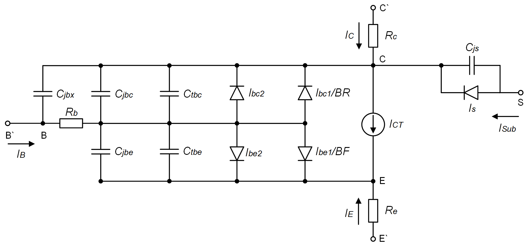
Fig. 1 Equivalent circuit diagram of the NPN bipolar transistor model#
Important
Depending on the value of the Transistor type property, the Substrate port can be grounded internally (Three-terminal) or exposed to the user (Four-terminal).
Note
The positive direction of currents is considered to be the direction into the transistor.
The following elements of the equivalent circuit and their designations are shown in Fig. 1:
\(R_b\) – base resistance connected between the external B` and internal B base nodes;
\(R_c\) – collector resistance connected between the external C` and internal C nodes of the collector;
\(R_e\) – emitter resistance, connected between the external E` and internal E emitter nodes;
\(I_{be1}\) – base-emitter junction current;
\(I_{be2}\) – base-emitter junction leakage current;
\(I_{bc1}\) – base-collector junction current;
\(I_{bc2}\) – base-collector junction leakage current;
\(I_s\) – substrate transition current;
\(I_{CT}=(I_{be1}-I_{bc1})/q_b\) – controlled source of collector transport current;
\(C_{jbc}\) – barrier capacitance of the base-collector junction;
\(C_{tbc}\) – diffusion capacitance of the base-collector junction;
\(C_{jbe}\) – barrier capacitance of the base-emitter junction;
\(C_{tbe}\) – diffusion capacitance of the base-emitter junction;
\(C_{js}\) – barrier capacitance of the substrate;
\(C_{jbx}\) is the barrier capacitance connected between the external base node B` and the internal collector node C.
The model parameters IS, IKF, ISE, IKR, ISC, ISS, IRB, CJC, CJE, CJS, ITF are multiplied by the AREA - relative transistor area property value, and the parameters RC, RE, RB, RBM are divided by it before being used in the equations below.
The dependence of the transport current IS on temperature is described by the formula (1) :
where:
\(VT=\frac{k \cdot T}{q}\) – thermal voltage, [V];
\(k\) – Boltzmann constant;
T – operating temperature of the transistor, [K];
q – elementary charge;
\(T_{NOM}\) – temperature at which the parameters of the transistor model were measured, [K];
\(EG\) – band gap width, [eV];
\(XTI\) – temperature coefficient for IS.
The dependence of saturation currents ISE, ISC, ISS on temperature is described by the formula (2):
where:
\(I\) – saturation current, [A];
\(N\) – emission coefficient (NE – for current ISE, NC – for current ISC, NS – for current ISS).
The dependence of the coefficients BF and BR on temperature is given in the formula (3):
where B is the maximum current transfer coefficient.
The dependence of resistances RE, RC, RB and RBM on temperature is described by the formula (4):
where:
\(R\) – resistance, [Ohm];
\(T1\) – linear temperature coefficient, [⁰C\(^{-1}\)] (TRE1 – for resistance RE, TRC1 – for resistance RC, TRB1 – for resistance RB, TRM1 – for resistance RBM);
\(T2\) – square temperature coefficient, [⁰C\(^{-2}\)] (TRE2 – for resistance RE, TRC2 – for resistance RC, TRB2 – for resistance RB, TRM2 – for resistance RBM).
The dependence of the band gap EG on temperature is described by the formula (5):
The dependence of contact potential differences VJE, VJC, VJS on temperature is determined by the formula (6):
where:
VJ – contact potential difference, [V];
EG(TNOM) – dependence of the band gap width on the temperature TNOM, determined by the formula (5);
EG(T) – dependence of the band gap width on temperature T, determined by the formula (5).
The dependence of the junction capacitances at zero bias CJE, CJC, CJS on temperature is determined by the formula (7):
where:
CJ – junction capacitance at zero bias, [F];
MJ – coefficient taking into account the smoothness of the transition (MJE – for CJE capacitance, MJC – for CJC capacitance, MJS – for CJS capacitance);
VJ(T) – dependence of the contact potential difference on temperature T (VJE(T) – for capacitance CJE, VJC(T) – for capacitance CJC, VJS(T) – for capacitance CJS), is determined by the formula (5).
Токи диодов \(I_{be1}\), \(I_{bc1}\), \(I_s\) в схеме замещения рассчитываются по формулам (8), (9), (10) в зависимости от значения напряжения на соответствующем переходе:
if U > 80 · N · VT (8) :
if U < -79 · N · VT (9) :
if -79 · N · VT ≤ U ≤ 80 · N · VT (10) :
where:
U – junction voltage (\(U_{be}\) – for current \(I_{be1}\), \(U_{bc}\) – for current \(I_{bc1}\), \(U_{sc}\) – for current \(I_s\));
I – saturation current (IS(T) – for currents \(I_{be1}\) and \(I_{bc1}\), ISS(T) – for current \(I_s\));
N – emission coefficient (NF – for current \(I_{be1}\), NR – for current \(I_{bc1}\), NS – for current \(I_s\)).
The leakage currents \(I_{be2}\), \(I_{bc2}\) in the equivalent circuit are calculated using the formulas (11), (12), (13) depending on the voltage value at the corresponding junction:
if U > 80 · N1 · VT (11) :
if U < -79 · N1 · VT (12) :
if -79 · N1 · VT ≤ U ≤ 80 · N1 · VT (13) :
where:
U – junction voltage (\(U_{be}\) – for current \(I_{be2}\), \(U_{bc}\) – for current \(I_{bc2}\));
I – saturation current (ISE(T) – for current \(I_{be2}\), ISC(T) – for current \(I_{bc2}\));
N1 – emission coefficient (NF – for current \(I_{be2}\), NR – for current \(I_{bc2}\));
N2 – leakage emission coefficient (NE – for current \(I_{be2}\), NC – for current \(I_{bc2}\)).
The base and collector currents (excluding capacitance currents) are found using the formulas (14) and (15), respectively:
where:
BF – maximum current transfer coefficient in normal mode;
BR – maximum current transfer coefficient in inverse mode;
\(q_b\) – normalized charge of the majority carriers in the base.
The normalized charge of the majority carriers in the base is calculated using the formulas (16), (17), (18) :[2]
where:
NK – gain roll-off coefficient at high currents;
VAF – Early voltage in normal mode, [V];
VAR – Early voltage in inverse mode, [V];
IKF – current at the beginning of the gain factor decline in normal mode, [A];
IKR – current at the beginning of the gain drop in the inverse mode, [A].
Note
When VAF = 0, VAR = 0, the Early effect in the direct and inverse modes is not taken into account, respectively.
When IKF = 0, IKR = 0, the effect of high current in the forward and inverse modes, respectively, is not taken into account.
The base resistance \(R_b\) depends on the value of the current IRB [2]:
if IRB = 0 (19) :
for IRB > 0 (20) :
where:
\(x=\frac{\sqrt{1+144\cdot I_b /(\pi^2\cdot IRB)}-1}{(24/ \pi^2)\cdot \sqrt{I_b/IRB}}\)
Note
When specifying a value for the RBM property, it must be less than or equal to RB. When RB = RBM, the base resistance is constant and independent of the IRB current.
The dependence of the charge transfer time through the base \(TF_{eff}\) is described by the formula (21) [2]:
where:
TF – ideal time of charge transfer through the base in normal mode, [s];
XTF – coefficient characterizing the dependence of the charge transfer time through the base on the base-collector junction bias;
ITF – current characterizing the dependence of the charge transfer time through the base on the collector current at high currents, [A];
VTF – voltage characterizing the dependence of the charge transfer time through the base on the base-collector junction bias, [V].
Note
When VTF = 0, the influence of voltage \(U_{bc}\) on the charge transfer time through the base is not taken into account.
Diffusion capacitances for the base-emitter and base-collector junctions are found using the formulas (22) and (23), respectively:
where TR is the ideal time of charge transfer through the base in inverse mode, [s].
Barrier capacitances \(C_{jbe}\), \(C_{jbc}\), \(C_{jbx}\) are determined by the formulas (24) and (25) according to the conditions [2]:
if U ≤ FC · VJ (24):
if U > FC VJ (25):
where:
FC – forward bias coefficient for junction capacitances;
U – junction voltage (\(U_{be}\) – for capacitance \(C_{jbe}\), \(U_{bc}\) – for capacitance \(C_{jbc}\), \(U_{b`c}\) – for capacitance \(C_{jbx}\)), [V];
VJ – junction voltage (\(U_{be}\) – for capacitance \(C_{jbe}\), \(U_{bc}\) – for capacitance \(C_{jbc}\), \(U_{b`c}\) – for capacitance \(C_{jbx}\)), [V].
Final values of the base-emitter, base-collector, and external base-collector capacitances (26), (27), (28):
where XCJC is the fraction of the diffusion capacitance connected between the internal nodes of the base and collector.
The barrier capacity of the substrate is calculated from the conditions:
if \(U_{sc}\) ≤ 0 (29):
if \(U_{sc}\) > 0 (30):
where:
\(U_{sc}\) – substrate voltage, [V];
CJS(T) – collector-substrate junction capacitance at zero bias, taking into account the temperature dependence, [F];
VJS(T) – contact potential difference of the collector-substrate junction taking into account the temperature dependence, [V];
MJS – coefficient taking into account the smoothness of the collector-substrate transition.
1. Properties#
Property |
Default Value |
Description |
Units of measurement |
|---|---|---|---|
Transistor type: |
Three-terminal |
– |
– |
1.0 |
– |
r.u. |
|
IS - transport saturation current |
1.0E-16 |
– |
А |
BF - ideal maximum forward beta |
100.0 |
– |
– |
NF - forward current emission coefficient |
1.0 |
– |
– |
VAF - forward Early voltage |
0.0 |
When set to 0, this parameter is excluded from the model equations |
V |
IKF - corner for BF high-current roll-off |
0.0 |
When set to 0, this parameter is excluded from the model equations |
А |
ISE - BE leakage saturation current |
0.0 |
– |
А |
NE - BE leakage emission coefficient |
1.5 |
– |
– |
BR - ideal maximum reverse beta |
1.0 |
– |
– |
NR - reverse current emission coefficient |
1.0 |
– |
– |
VAR - reverse Early voltage |
0.0 |
When set to 0, this parameter is excluded from the model equations |
V |
IKR - corner for BR high-current roll-off |
0.0 |
When set to 0, this parameter is excluded from the model equations |
А |
ISC - BC leakage saturation current |
0.0 |
– |
А |
NC - BC leakage emission coefficient |
2.0 |
– |
– |
NK - high-current roll-off coefficient |
0.5 |
– |
– |
ISS - substrate junction saturation current |
0.0 |
– |
А |
NS - substrate junction emission coefficient |
1.0 |
– |
– |
RB - zero bias base resistance |
0.0 |
– |
Ohm |
RBM - minimum base resistance at high currents |
0.0 |
RBM must be less than or equal to RB. When RBM = RB, base resistance is constant. |
Ohm |
IRB - current at which base resistance is (RB+RBM)/2 |
0.0 |
– |
А |
RE - emitter resistance |
0.0 |
– |
Ohm |
RC - collector resistance |
0.0 |
– |
Ohm |
FC - forward-bias depletion capacitor coefficient |
0.5 |
– |
– |
CJE - BE zero-bias depletion capacitance |
0.0 |
– |
F |
VJE - BE junction built-in potential |
0.75 |
– |
V |
MJE - BE junction grading coefficient |
0.33 |
– |
– |
TF - ideal forward transit time |
0.0 |
– |
s |
XTF - coefficient for bias dependence of TF |
0.0 |
– |
– |
VTF - transit time dependence on VBC |
0.0 |
When set to 0, this parameter is excluded from the model equations |
V |
ITF - high current dependence of TF |
0.0 |
When set to 0, this parameter is excluded from the model equations |
А |
CJC - BC zero-bias depletion capacitance |
0.0 |
– |
F |
VJC - BC junction built-in potential |
0.75 |
– |
V |
MJC - BC junction grading coefficient |
0.33 |
– |
– |
TR - ideal reverse transit time |
0.0 |
– |
s |
XCJC - fraction of CJC capacitance connected to internal base |
1.0 |
– |
– |
CJS - CS zero-bias depletion capacitance |
0.0 |
– |
F |
VJS - CS junction built-in potential |
0.75 |
– |
V |
MJS - CS junction grading coefficient |
0.0 |
– |
– |
T - transistor operating temperature |
27.0 |
– |
°C |
Tnom - temperature at which the model parameters were measured |
27.0 |
– |
°C |
EG - energy gap |
1.11 |
– |
eV |
XTI - IS temperature effect exponent |
3.0 |
– |
– |
XTB - BF and BR temperature coefficient |
0.0 |
– |
– |
TRE1 - RE linear temperature coefficient |
0.0 |
– |
°C⁻¹ |
TRE2 - RE quadratic temperature coefficient |
0.0 |
– |
°C⁻² |
TRB1 - RB linear temperature coefficient |
0.0 |
– |
°C⁻¹ |
TRB2 - RB quadratic temperature coefficient |
0.0 |
– |
°C⁻² |
TRM1 - RBM linear temperature coefficient |
0.0 |
– |
°C⁻¹ |
TRM2 - RBM quadratic temperature coefficient |
0.0 |
– |
°C⁻² |
TRC1 - RC linear temperature coefficient |
0.0 |
– |
°C⁻¹ |
TRC2 - RC quadratic temperature coefficient |
0.0 |
– |
°C⁻² |
2. Inputs and outputs#
Parameters |
Input/Output |
Description |
Units of measurement |
Port type |
|---|---|---|---|---|
Base |
Input |
- |
- |
Electronics |
Collector |
Input |
- |
- |
Electronics |
Input |
Available when |
- |
Electronics |
|
Emitter |
Output |
- |
- |
Electronics |
Для того, чтобы посмотреть возможности подключения блока необходимо перейти на страницу Описание портов блоков