

IGBT#
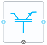
Block appearance in REPEAT VISION#
The IGBT block is a simplified model of an insulated gate bipolar transistor. The circuit for replacing such transistor consists of a key that determines the transistor resistance (when activated, it is equal to the internal resistance, and when deactivated, it is equal to the resistance in the closed state) depending on the logic signal (if 1 is applied to the control input and voltage on the transistor is greater than the value of forward bias voltage, the transistor is open; if any of the above conditions are not met, the transistor is deactivated). Equivalent circuit of bipolar transistor with isolated gate and its CVD is given in figures below Fig. 1 and Fig. 2.
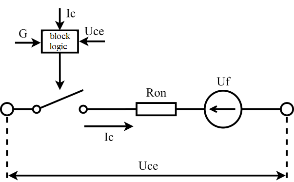
Fig. 1 Circuit of isolated gate bipolar transistor replacement#
In this circuit:
G - control signal (can take a value equal to either 0 or 1; 0 corresponds to the closed position of the transistor and 1 to the open position);
\(I_c\) - collector current value, [А];
\(U_{ce}\) - voltage between collector and emitter, [V];
\(R_{on}\) - resistance of transistor in open state, [Ohm];
\(U_f\) - forward bias voltage of transistor p-n movement, [V].
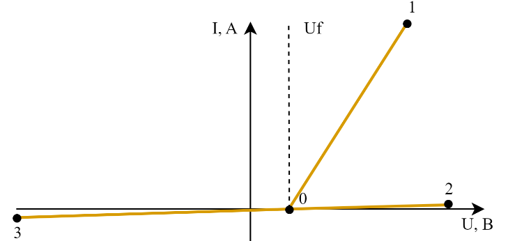
Fig. 2 CVD of insulated gate bipolar transistor#
CVD of an insulated gate bipolar transistor reflects the logic of its operation. So, when voltage is applied between the collector and the emitter, less than \(U_f\), the transistor will be in a closed state, regardless of the control signal magnitude. The 0-3 CVD section corresponds to such conditions. The CVD slope in this case is determined by the value of the set resistance in the closed state. If voltage is supplied greater than \(U_f\) and a control action is equal to 1, the transistor opens and is described by the 0-1 section of the CVD. The CVD slope in this case is determined by \(R_{on}\). When voltage is supplied greater than \(U_f\) and a control action is equal to 0, the transistor closes and is described by the 0-2 section of the CVD. The CVD slope in this case is determined by the transistor resistance in the closed state.
1. Properties#
Property |
Default Value |
Description |
Units of measurement |
|---|---|---|---|
Internal resistance |
1e-3 |
- |
Ohm |
Turn-off resistance |
1e12 |
- |
Ohm |
Forward voltage |
1 |
- |
V |
On |
- |
- |
|
Snubber resistance |
1e6 |
Available, when |
Ohm |
Snubber capacitance |
1e9 |
Available, when |
F |
2. Inputs and outputs#
Parameters |
Input/Output |
Description |
Units of measurement |
Port type |
|---|---|---|---|---|
Control input |
Input |
- |
- |
Automation |
Collector |
Input |
- |
- |
Electronics |
Emitter |
Output |
- |
- |
Electronics |
In order to see the connection capabilities of the block, you need to go to page Description of block ports