

MOSFET n-type (SPICE model)#

Block appearance in REPEAT VISION#
The MOSFET n-type (SPICE model) block is a SPICE model of an n-type MOSFET that implements one version of the model (level 1). The block implements the following equivalent circuit:
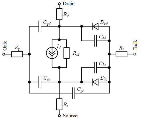
Substitution scheme#
Thermal stress is calculated using the formula (1):
where:
\(k\) – Boltzmann constant, \(k=1.38 \cdot 10^{-23}\) [J/K];
\(T\) - diode temperature, [K];
\(q\) is the elementary electric charge of an electron, \(q=1.602 \cdot 10^{-19}\) [C].
Below are the equations for the first-level MOSFET model of direct drain-source voltage polarity.
When calculating gate capacitances, the equations (2) are used:
Shutter capacities are calculated using the formulas:
accumulation region (\(V_{gs}\) < \(V_{th}\) – \(PHI\)) (3):
depletion region (\(V_{on}\) – \(PHI\) < \(V_{gs}\) < \(V_{th}\)) (4):
saturation region (\(V_{th}\) < \(V_{gs}\) < \(V_{th}\)+\(V_{ds}\)) (5):`:
linear region (\(V_{gs}\) > \(V_{th}\)+\(V_{ds}\)) (6):
When calculating the transition regions, the equations are used (7) :
Transition capacitances are calculated using the formulas:
with \(CBS\)=0 and \(CBD\)=0 (8):
for \(CBS\)>0 and \(CBD\)>0 (9):
When calculating the main current of a transistor, the equation is used (10):
The main current of the transistor is calculated using the formulas:
cutoff region
{eq}ElectronicSpiceMosfetNMOS11`:
linear region (12):
saturation region (13):
1. Properties#
Property |
Default Value |
Description |
Units of measurement |
|---|---|---|---|
L – channel length |
1E-4 |
– |
m |
W – channel width |
1E-4 |
– |
m |
AD - area of drain |
0.0 |
– |
m\(^2\) |
AS – area of source |
0.0 |
– |
m\(^2\) |
RDS – drain-source shunt resistance |
1E6 |
– |
Ohm |
RD – drain ohmic resistance |
0.0 |
– |
Ohm |
RS – source ohmic resistance |
0.0 |
– |
Ohm |
RG – gate ohmic resistance |
0.0 |
– |
Ohm |
RB – bulk ohmic resistance |
0.0 |
– |
Ohm |
CGDO – gate-drain overlap cap. |
0.0 |
– |
F/m |
CGSO – gate-source overlap cap. |
0.0 |
– |
F/m |
CGBO – gate-bulk overlap cap. |
0.0 |
– |
F/m |
CBD – bulk p-n zero-bias B-D cap. |
0.0 |
– |
F |
CBS – bulk p-n zero-bias B-S cap. |
0.0 |
– |
F |
CJ – bulk p-n zero-bias bot. cap. |
0.0 |
– |
F/m\(^2\) |
CJSW – bulk p-n zero-bias s/w cap. |
0.0 |
– |
F/m |
MJ – bulk p-n zero-bias bottom grad. |
0.5 |
– |
– |
MJSW – bulk p-n zero-bias s/w coeff. |
0.33 |
– |
– |
TT – bulk p-n transit time |
0.0 |
– |
s |
IS – bulk p-n saturation current |
1E-14 |
– |
– |
PB – bulk p-n bottom potential |
0.8 |
– |
V |
PBSW – bulk p-n sidewall potential |
0.8 |
– |
V |
FC – forward-bias depletion coeff. |
0.5 |
– |
– |
LD – lateral diffusion length |
0.0 |
– |
m |
KP – process transconductance |
2E-5 |
– |
A/V\(^2\) |
VTO – zero-bias threshold voltage |
0.0 |
– |
V |
GAMMA – body-effect coefficient |
0.0 |
– |
В\(^{0.5}\) |
PHI – surface inversion potential |
0.6 |
– |
V |
LAMBDA – channel-length modulation |
0.0 |
– |
V\(^-1\) |
TOX – gate oxide thinkness |
1E-7 |
– |
m |
T – transistor temperature |
300 |
– |
К |
2. Inputs and outputs#
Parameters |
Input/Output |
Description |
Units of measurement |
Port type |
|---|---|---|---|---|
Drain |
Input |
- |
- |
Electronics |
Gate |
Input |
- |
- |
Electronics |
Source |
Output |
- |
- |
Electronics |
Bulk |
Output |
- |
- |
Electronics |
In order to see the connection capabilities of the block, you need to go to page Description of block ports