

GaAsFET (SPICE model)#

Block appearance in REPEAT VISION#
The GaAsFET (SPICE model) block is a SPICE model of a gallium arsenide field-effect transistor that implements three model levels. The block implements the following equivalent circuit, shown in Fig. 1:
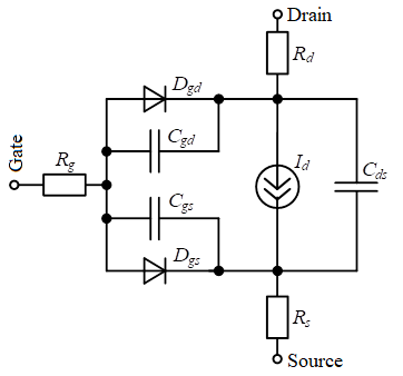
Fig. 1 Equivalent circuit#
Thermal stress is calculated using the formula (1):
where:
\(k\) – Boltzmann constant, \(k=1.38 \cdot 10^{-23}\) [J/K];
\(T\) – diode temperature, [K];
\(q\) is the elementary electric charge of an electron, \(q=1.602 \cdot 10^{-19}\) [C].
Current \(I_d\) is calculated using the formulas:
For the first level model (Level 1):
cutoff region (\(U_{gs}\) ≤ VTO) (2) :
linear region and saturation region (\(U_{gs}\) > VTO) (3) :
For the second level model (Level 2):
For the third level model (Level 3):
The equivalent circuit capacitances are calculated using the formulas:
For the first level model (Level 1) (6) :
For Level 2 and Level 3 models (7) :
1. Properties#
Property |
Default Value |
Description |
Units of measurement |
|---|---|---|---|
Level of model: |
Level 1 |
– |
– |
AREA - device area |
1.0 |
– |
– |
VTO - pinch-off voltage |
-2.5 |
– |
V |
ALPHA - saturation voltage parameter |
2.0 |
– |
V\(^{-1}\) |
BETA - transconductance coefficient |
0.1 |
– |
А/V\(^2\) |
B - doping tail extender |
0.3 |
– |
V\(^{-1}\) |
LAMBDA - channel-length modulation |
0.0 |
– |
V\(^{-1}\) |
GAMMA - static feedback parameter |
0.0 |
– |
– |
DELTA - output feedback parameter |
0.0 |
– |
V\(^{-1}\) |
Q - power law parameter |
2.0 |
– |
– |
RG - gate ohmic resistance |
0.0 |
– |
Ohm |
RD - drain ohmic resistance |
0.0 |
– |
Ohm |
RS - source ohmic resistance |
0.0 |
– |
Ohm |
IS - gate pn saturation current |
1.0E-14 |
– |
А |
N - gate pn emission coefficient |
1.0 |
– |
– |
M - gate pn grading coefficient |
0.5 |
– |
– |
VBI - gate pn potential |
1.0 |
– |
V |
CGD - zero-bias gate-drain pn cap. |
1.0E-9 |
– |
F |
CGS - zero-bias gate-source pn cap. |
1.0E-9 |
– |
F |
CDS - fixed drain-source cap. |
1.0E-9 |
– |
F |
FC - forward-bias depletion coeff. |
0.5 |
– |
– |
VDELTA - capacitance transition volt. |
0.2 |
– |
V |
VMAX - capacitance limiting voltage |
0.5 |
– |
V |
EG - bandgap voltage |
1.12 |
– |
eV |
XTI - temperature coefficient of IS |
0.0 |
– |
– |
VTOTC - temperature coefficient of VTO |
0.0 |
– |
V/°C |
BETATCE - exp. temperature coeff. of BETA |
0.0 |
– |
%/°C |
TRG1 - temperature coefficient of RG |
0.0 |
– |
°C⁻¹ |
TRD1 - temperature coefficient of RD |
0.0 |
– |
°C⁻¹ |
TRS1 - temperature coefficient of RS |
0.0 |
– |
°C⁻¹ |
T - device operating temperature |
27.0 |
– |
°C |
Tnom - temperature at which the model parameters are measured |
27.0 |
– |
°C |
2. Inputs and outputs#
Parameters |
Input/Output |
Description |
Units of measurement |
Port type |
|---|---|---|---|---|
Drain |
Input |
- |
- |
Electronics |
Gate |
Input |
- |
- |
Electronics |
Source |
Output |
- |
- |
Electronics |
In order to see the connection capabilities of the block, you need to go to page Description of block ports